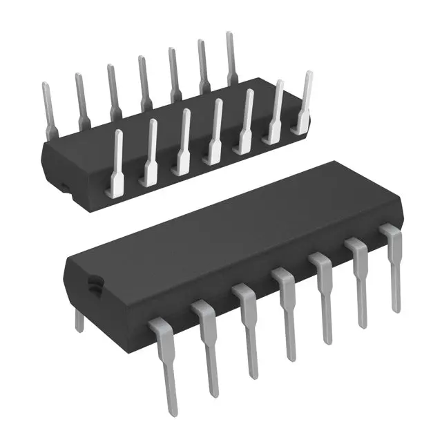
Description
CD4011 NAND gates provide the system designer with direct implementation of the NAND function and supplement the existing family of CMOS gates. All inputs and outputs are buffered.
Applications:
- Clock & Timing
- Consumer Electronics
Features:
- Propagation delay time = 60ns Typ. at CL = 50pF, VDD = 10 V
- Buffered inputs and outputs
- Standardized symmetrical output characteristics
- Maximum input current of 1A at 18V over full package temperature range; 100nA at 18V and 25C
- 100% tested for quiescent current at 20V
Explore more from our collection.
Reviews
There are no reviews yet.